![]()
![]()
![]()
|
|
|
|
8088 Microprocessor Project
Apparatus
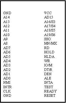
Wire rapper, Striper, Connecting Wires , Soldering Iron, Soldering wire, Digital Multimeter, nose plask ,I/O Board, IC, IC Holder, Power Supply. Power Supply A 5 volt regulated power supply is constructed with a Transformer, Capacitor (1000m f/22000m f), Viroboard, Wire and 7805 IC, which provide 5 volts. Description of 8088 Microprocessor The 8088 microprocessor are packaged in 40-pin dual in line package(DIPS). 8088 is a 16 bit microprocessor with an 8-bit data bus. 8088 has pin connections AD0-AD7. 8088 data bus has a difference of microprocessor with others. 8088 has a IO/M pin. 8088 requires +5.0 volts with a supply voltage tolerance of +-10 percent. 8088 draws a maximum of 340mA. It can operate in ambient temperature of between 32-180 F.The ground connection is the return for the power supply. The 8088 have two pins labeled GND both must be connected to ground for proper operation. It use the memory and I/O in periods of time called BUS CYCLE. It can write data or read data between at a maximum rate of 1.25 million times per second. Minimum mode operation is obtained by connecting the mode selection pin MN/MX to +5.0volts, and maximum mode is selected by grounding the pin. Whenever 8088 microprocessor are reset, they begin executing the software at memory location FFFF0H (FFFF:0000) with the interrupt request pin disable. Input characteristic of the 8088 microprocessor
Output characteristic of the 8088 microprocessor
8088 Mother Board consist of the following IC 8088 (Micro processor)
74LS245 74LS373 8251A 74LS62256 74LS2764 74LS00 8284A 8088 Description of ICs 8284a (clock generator) 8284a is a clock generator IC. It has the following pins: AEN1 and AEN2: use to provide bus Ready signal (i.e. to enable RDY1 and RDY2) signals RDY1 and RDY2: These provide bus ready signals in conjunction with AEN1 And AEN2. ASYNC: It select input, either one or two stages of RDY1 and RDY2. READY: READY is an out put pin that connects to 8088 Ready pin. X1 and X2: It is an external crystal use as timing source for clock generation. F/C: It provides timing signal. EFI: It supplies the timing signal whenever the f/c pin is high. CLK: The clock output pin provides the clock-input signal to 8088 microprocessor. PCLK: It provides a clock signal to peripheral devices in the system. OSC: It’s output it’s a TTL level signal. RES: The reset input is an active low .pin is often to an RC network RESET: It output is connected to 8088 reset input pin. CSYNC: Pin is used whenever EFI input provides synchronization pin is used. GND: The ground pin connects to ground. VCC: This power supply pin connects to +5.0 volts with a tolerance of +-10%. 74LS245:It is Octal Bi directional Bus Buffer. 74LS373:It is a transparent Latch. 62256: It is a 32k static RAMS which are interfaced to 8088 microprocessor. 2764: It is a EPROM for a 64k memory in an 8088 microprocessor base system(it is memory based device). 74LS00:Quad 2-input NAND gate. |